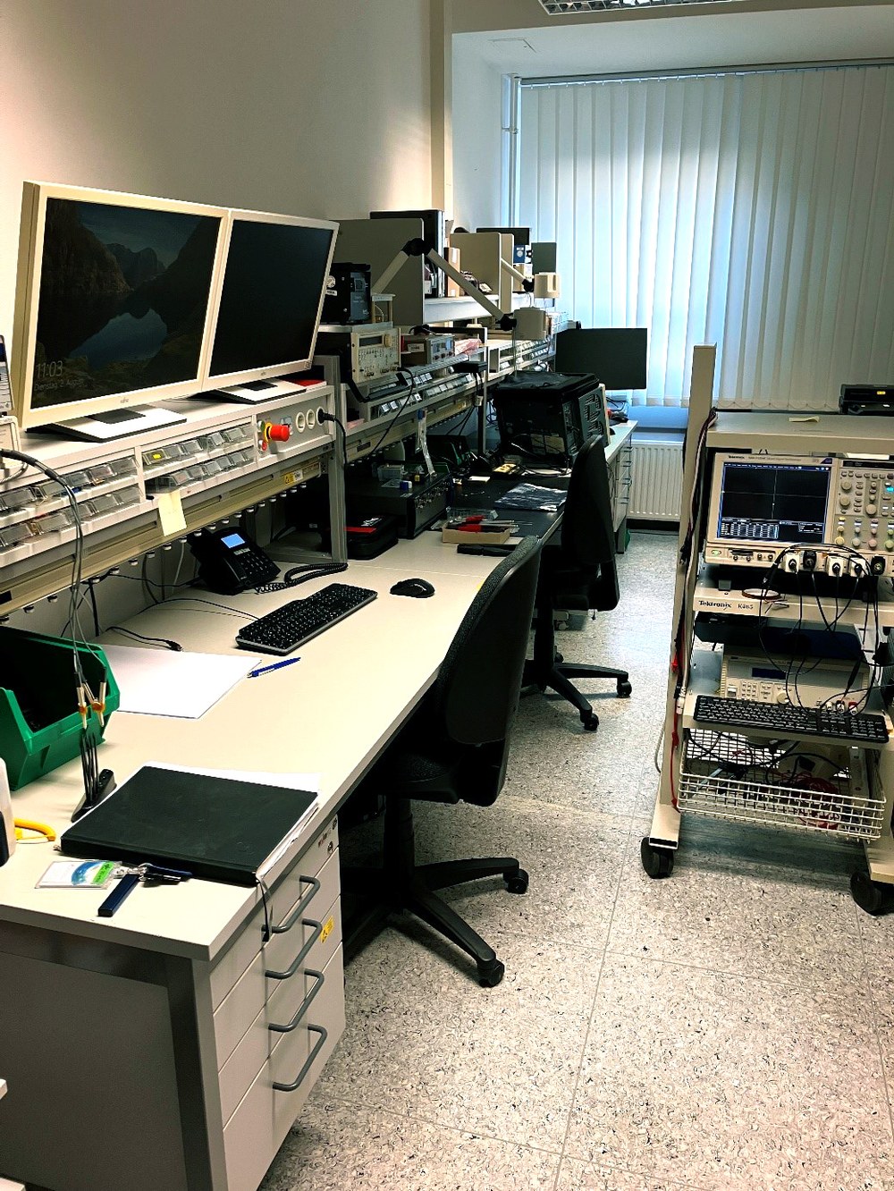
CCD- Laboratory

The main focus of this laboratory is the commissioning of focal plane electronics for various projects. The small CCD laboratory has three workspaces for electronical work – all equipped with ionizers, providing ion balance adjustment and ion level alarm output. Protection against electro static discharge is given by conductive flooring, chairs and desktop, providing best possible environment for all kinds of CCD sensor equipment.
It is suitable for debugging engineering model circuitry and breadboard setups, such as the CMOS-TDI T89022A test chip, which electro-optical verification started in this room. Additionally, it is suitable for pre-integration tests of flight model PCBs, as done at the project KompSat 7 (KARI), the same steps will be performed for EOIR project (KARI). In the latter projects, long-term stability tests for sensitive circuitry, worst case loading tests and noise measurements were performed to verify the design.
For electrical measurement and verification, a 12.5 Gigahertz (GHz) oscilloscope and an AF spectrum analyser (1 Megahertz (MHz)) are used beside various conventional laboratory equipment. In addition, simple radiometric tests can be performed – measurements like linearity or photon transfer curves for pre-integration test purpose.
