Scanning Electron Microscopes (SEM)

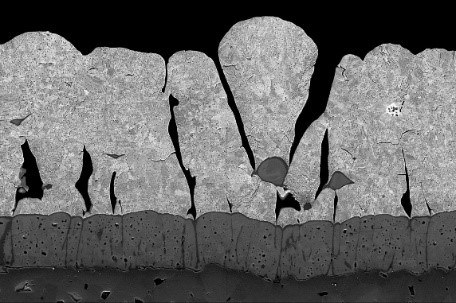
The scanning electron microscope is used to image and analyze the surface of a sample. When examining fractured or cut surfaces and metallographically prepared sample surfaces, depending on the selected sample orientation, not only surface information but also information about the internal structure of the sample can be obtained. The scanning electron microscope allows for a higher spatial resolution than a light microscope.
Today, scanning electron microscopy (SEM) is one of the fundamental characterization methods in materials science. Qualitative and quantitative information on topology as well as phase inventory, phase fractions and orientations are obtained through the installed detectors. Imaging of fracture surfaces for analysis and in-situ observations under mechanical stress are also part of the scanning electron microscopy repertoire.
Energy dispersive X-ray spectroscopy (EDX) enables qualitative and quantitative chemical analysis, while backscattered electron diffraction (EBSD) provides texture information as a method for orientation determination on a microscopic scale.
The institute runs two scanning electron microscopes:
Zeiss Ultra 55:
- Field emission cathode, resolving power at 15 kV and above 1 nm; at 1 kV 1.7 nm.
- Secondary electron and backscattered electron detectors (SE and BSE detectors), each in chamber and "in-lens" versions.
- Oxford AZtec EDX- system with beam control for automated measurement (line scan, mapping).
- Oxford Channel5 / Nordlys II EBSD system.
- In-situ module for tensile and compression tests from Kammrath & Weiss.
- MBX bending module 500N from Kammrath & Weiss
Hitachi HU3900:
- Tungsten cathode, resolving power at 30 kV 3 nm; at 1 kV 15 nm.
- Secondary electron and backscattered electron detectors, low vacuum secondary electron detector.
- Low vacuum mode at pressures from 6 Pa - 650 Pa
- Large sample chamber for samples up to 20 cm diameter, 13 cm height and 5 kg weight.
- Software for 3D surface reconstruction (Hitachi map 3D).
- Software for automated image acquisition (Hitachi Multi ZigZag).
- Oxford AZtecLive EDX- system with beam control for automated measurement (line scan, mapping).
